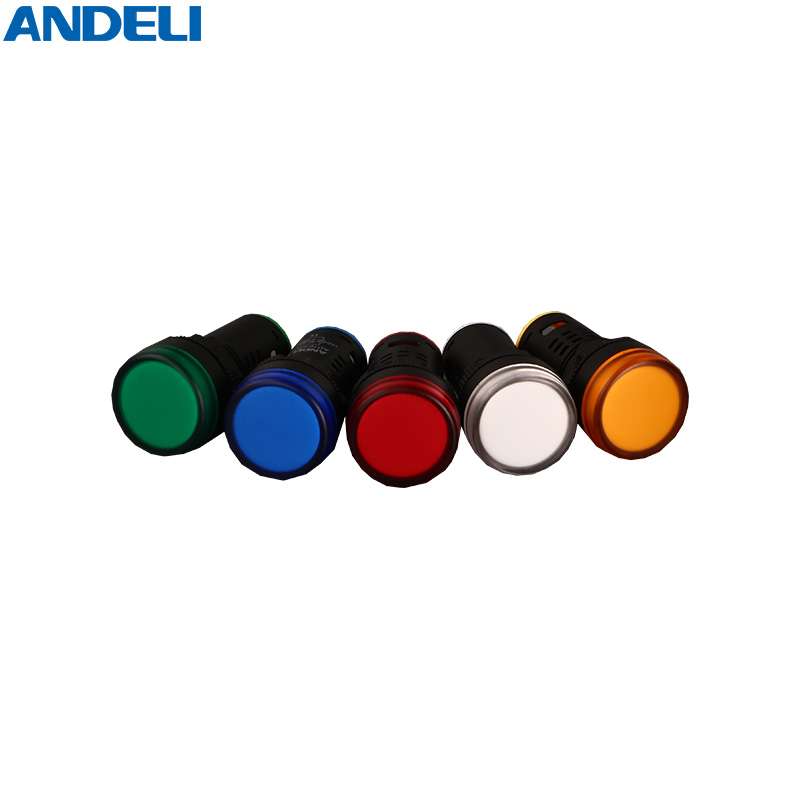
Optoelectronic Devices
Source high-quality optoelectronic devices from vetted suppliers and manufacturers in China and across Asia. Designed for electronics importers, wholesale distributors, and OEMs, our network provides reliable bulk production and custom manufacturing. Secure competitive pricing and stringent quality control for your component supply chain.
Optoelectronic devices form the critical interface between electrical and optical signals in modern hardware. Sourcing these components in bulk requires navigating complex binning systems, strict thermal management specifications, and highly variable yield tolerances. For procurement managers and OEMs, the primary challenge when importing from overseas manufacturers is ensuring strict consistency in wavelength, luminosity, and forward voltage across multiple production batches.
Critical Specifications and Binning
When negotiating with optoelectronic manufacturers, the datasheet is only the starting point. Factory yields naturally produce components with varying characteristics, which are sorted into "bins." Failing to specify acceptable bins in your purchase order will result in shipments containing mixed performance profiles.
Key Specifications to Define in Your PO
- Wavelength (nm) tolerances: Specify exact peak and dominant wavelength ranges to ensure color/signal consistency.
- Forward Voltage (Vf) bins: Tightly controlled Vf bins are essential for parallel circuit designs to prevent thermal runaway.
- Luminous/Radiant Flux: Define minimum and maximum output thresholds at your specified drive current.
- Thermal Resistance (Rth): Crucial for high-power devices to ensure long-term reliability and minimize degradation.
- Viewing Angle / Beam Divergence: Specify the required optical distribution pattern and acceptable deviation.
Struggling with inconsistent optical performance across production batches? We help buyers standardize their supply chain and enforce strict binning requirements.
Talk to our teamManufacturing Processes and Quality Control
The reliability of an optoelectronic component is determined during the highly sensitive packaging and bonding phases. Even if a factory purchases premium semiconductor die, poor assembly environments will introduce microscopic defects that drastically reduce the component's lifespan.
Die Bonding
The semiconductor die is attached to the lead frame or substrate. Voids in the conductive epoxy here increase thermal resistance, leading to early failure.
Wire Bonding
Gold or copper wires connect the die to the electrical leads. Improper tension or poor bond quality results in intermittent connections under thermal cycling.
Encapsulation
Optical-grade silicone or epoxy is applied. Moisture trapped during this phase, or improper curing, causes lens yellowing and catastrophic failure during reflow soldering.
To mitigate these risks, implementing rigorous Quality Control & Inspection protocols is non-negotiable. Pre-shipment inspections must include integrating sphere testing for optical properties and thermal shock testing for mechanical reliability.
Moisture Sensitivity Levels (MSL)
Optoelectronic devices packaged in clear resins are highly susceptible to moisture absorption. Ensure your supplier bakes the components and vacuum-seals them with desiccant according to JEDEC J-STD-033 standards. Failure to do so will result in "popcorning" defects during your PCB assembly process.
Compliance and Supplier Vetting
Navigating the landscape of Asian component manufacturers requires distinguishing between actual packaging facilities, die fabricators, and trading companies. Conducting thorough Factory Audits ensures your chosen supplier has the necessary cleanroom environments (Class 10,000 or better) and automated sorting equipment.
Furthermore, depending on your target market and application, specific certifications are required. Working with a partner who understands Compliance & Testing helps verify that your components meet global standards.
| Requirement | Standard Commercial | Industrial / Automotive |
|---|---|---|
| Operating Temperature | -20°C to 85°C | -40°C to 125°C |
| Reliability Standard | JESD22 | AEC-Q102 |
| Environmental | RoHS / REACH | RoHS / REACH / Conflict Minerals |
Pricing, MOQs, and Lead Times
Pricing in the optoelectronics market is heavily driven by raw material costs (like gold wire and specialized substrates), die size, and the strictness of your binning requirements. Requesting a single, tight bin will cost significantly more than accepting a wider distribution, as the factory must absorb the cost of the unused yield.
Need to negotiate better terms or consolidate your component sourcing? Let our procurement experts evaluate your current BOM.
Get a free consultationFrequently Asked Questions
Sourcing optoelectronic devices at scale demands strict oversight of manufacturing environments and a deep understanding of optical specifications. By controlling binning parameters and enforcing rigorous quality standards at the factory level, buyers can ensure consistent performance while maintaining competitive margins.
Get Sourcing Help for Optoelectronic Devices
Tell us your requirements and our experts will connect you with verified manufacturers.