Multilayer PCB
Source high-quality multilayer PCBs directly from vetted manufacturers and factories. Built for importers, electronics distributors, and brands requiring reliable OEM production, our network delivers strict impedance control, advanced HDI capabilities, and IPC-compliant manufacturing at wholesale volumes.
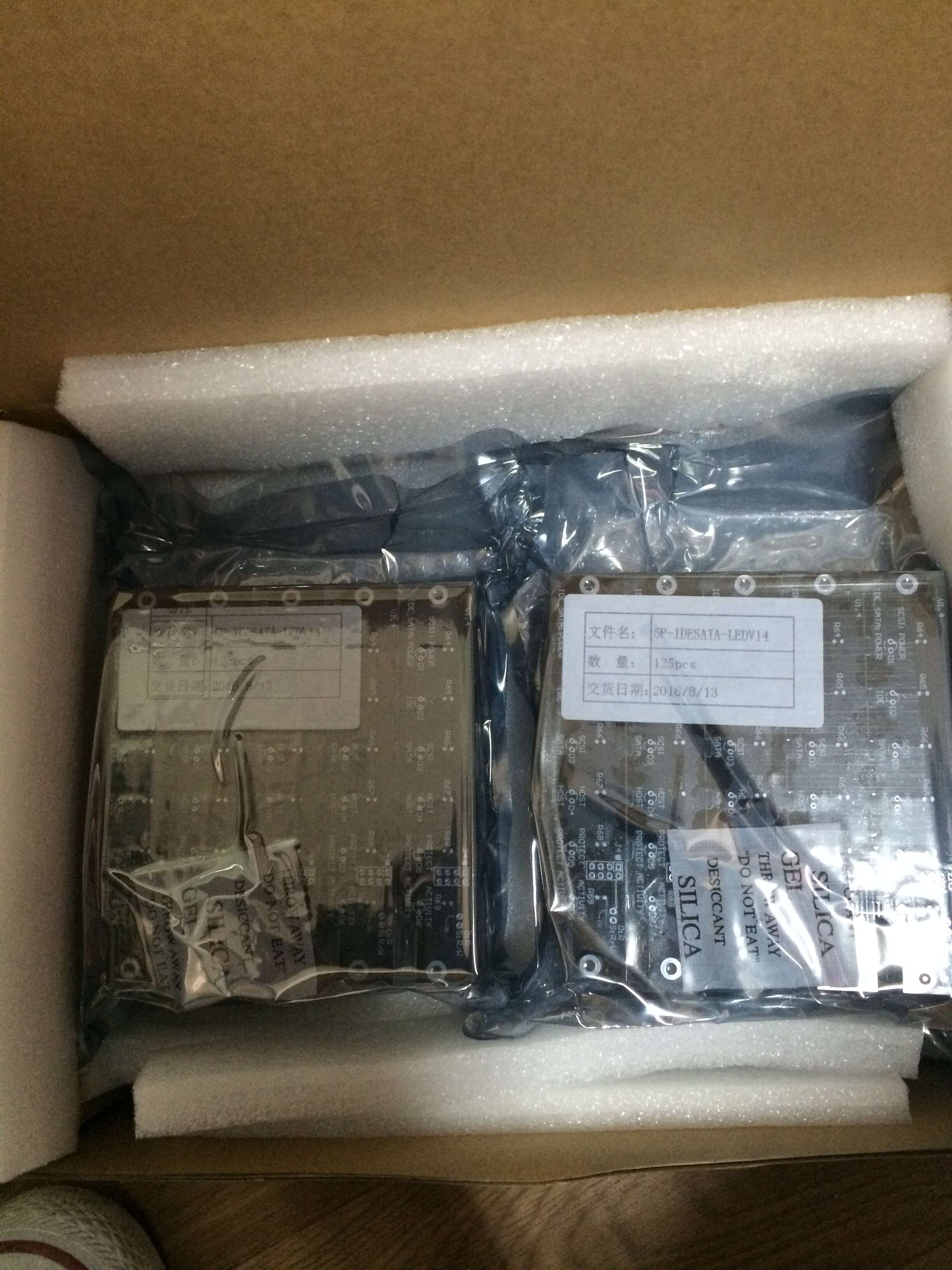
Multilayer PCBs form the critical backbone of modern high-density electronics, from telecommunications infrastructure to automotive control systems. When scaling from prototype runs to wholesale volume production, the sourcing equation changes dramatically. The focus must shift from rapid turnaround times to yield stability, material integrity, and strict factory process control. A minor alignment error in a 12-layer stackup or a substituted dielectric material can compromise an entire production run.
To successfully source multilayer boards in bulk, buyers must lock down precise specifications and ensure the manufacturing partner possesses the heavy equipment and quality management systems required for complex lamination and drilling.
Core Specifications for Volume Production
When requesting quotes for multilayer boards, generic specifications lead to highly variable pricing and inconsistent performance. Factories need precise data to calculate material utilization and process time.
Beyond standard dimensions and layer count, your Gerber files and fabrication notes must explicitly define:
- Dielectric Material & Tg Rating: Standard FR4 (Tg 130-140C) is sufficient for basic consumer goods, but industrial or automotive applications require High-Tg FR4 (Tg 170C and above) to withstand thermal stress during assembly and operation.
- Copper Weight: Specify inner and outer layer copper separately (e.g., 1oz inner, 2oz outer). Heavy copper boards require specialized etching processes to prevent undercutting.
- Impedance Control: If your design includes high-speed signals (USB, HDMI, PCIe), you must specify the target impedance and acceptable tolerance (typically plus or minus 10 percent).
- Surface Finish: The finish impacts both shelf life and assembly yield.
| Surface Finish | Shelf Life | Best Application | Cost Profile |
|---|---|---|---|
| HASL (Lead-Free) | 12 months | General consumer electronics | Low |
| ENIG | 12 months | Fine pitch BGA, wire bonding | High |
| OSP | 6 months | High-volume, flat pad requirements | Low |
| Immersion Silver | 6-12 months | High-speed signals, RF | Medium |
Need help matching your board specifications to the right tier of manufacturer? We match your DFM requirements with vetted facilities.
Talk to our teamManufacturing Tolerances and Factory Capabilities
The transition from a 2-layer to a 4-layer or 8-layer board introduces the lamination process. Layers of prepreg and copper core must be bonded under extreme heat and pressure. This is where lower-tier factories struggle.
Poor lamination leads to delamination during wave soldering. Inaccurate mechanical drilling causes via registration failures, where the drill bit misses the internal copper pads, leading to open circuits. Before committing to a volume order, it is highly recommended to conduct rigorous Factory Audits to verify their equipment baseline.
Critical Factory Capabilities to Verify
- In-house lamination presses (outsourcing this step introduces massive quality risks)
- Laser Direct Imaging (LDI) equipment for precise trace resolution under 3 mil
- Automated Optical Inspection (AOI) performed on all inner layers prior to lamination
- Time Domain Reflectometer (TDR) testing capabilities for impedance control verification
- Vacuum plugging equipment for via-in-pad requirements
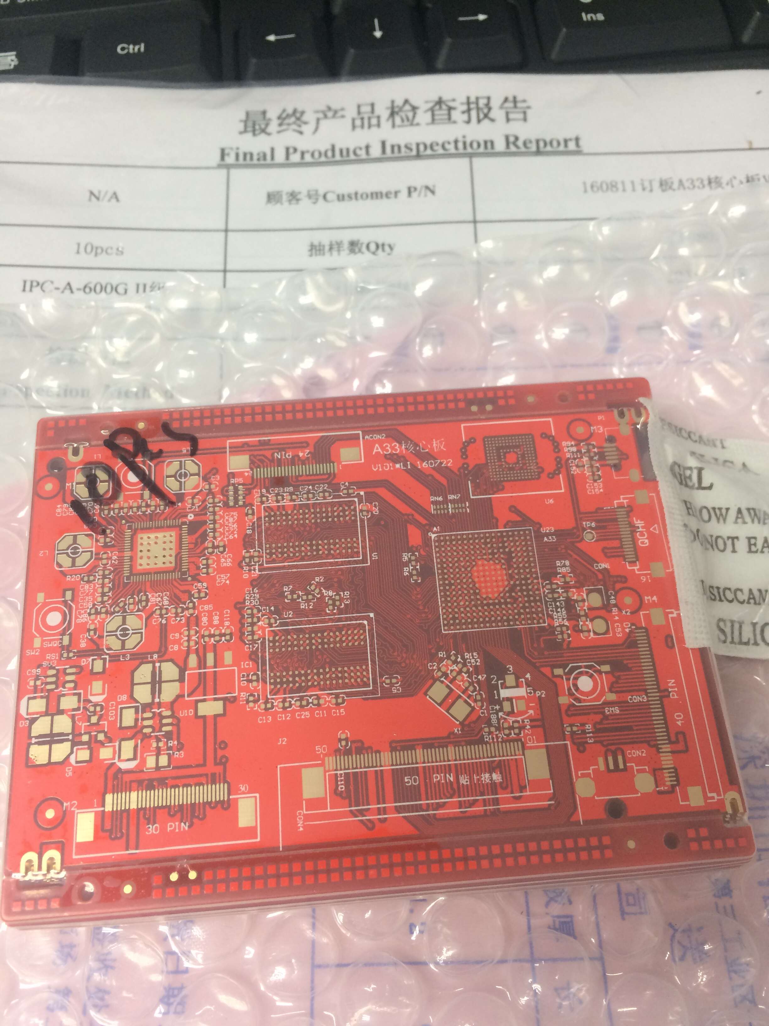
Quality Control and Testing
Never accept a bulk PCB order without 100 percent electrical testing. For volume production, factories should use custom test fixtures (bed-of-nails) rather than flying probe testers, which are too slow for mass production. Implementing independent Quality Control & Inspection ensures that the factory provides cross-section analysis reports and solderability test results before the boards leave the facility.
Pricing, MOQs, and Production Lead Times
Multilayer PCB pricing is heavily dependent on panel utilization. A board size that wastes 30 percent of the standard copper clad laminate panel will artificially inflate your unit cost. Engaging in Product Development and DFM (Design for Manufacturing) reviews with the factory can often optimize the board dimensions to maximize panel yield.
Optimize your PCB supply chain. We negotiate tooling costs, manage quality control, and handle all international logistics.
Get a free consultationFrequently Asked Questions
Securing a reliable supply of multilayer PCBs is about balancing technical capability with scalable pricing. The unit cost is only one factor; yield rates, material authenticity, and consistent on-time delivery ultimately dictate your total cost of ownership. Working with an experienced sourcing partner ensures your manufacturing baseline is secure from the first test run to full-scale production.
Get Sourcing Help for Multilayer PCB
Tell us your requirements and our experts will connect you with verified manufacturers.