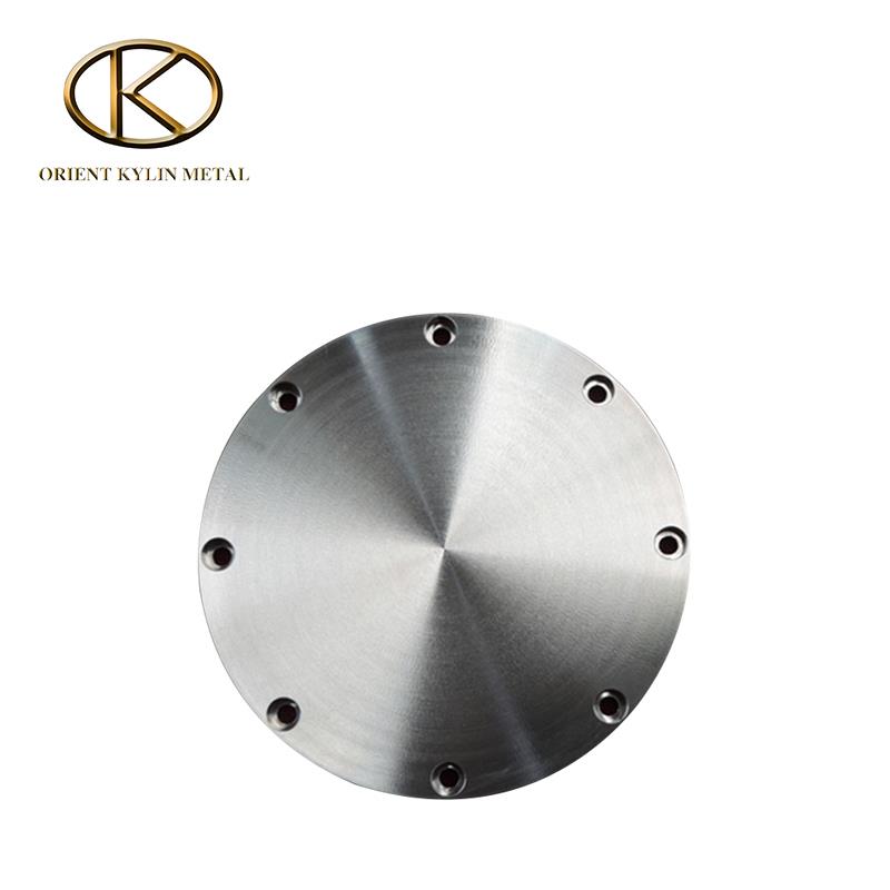
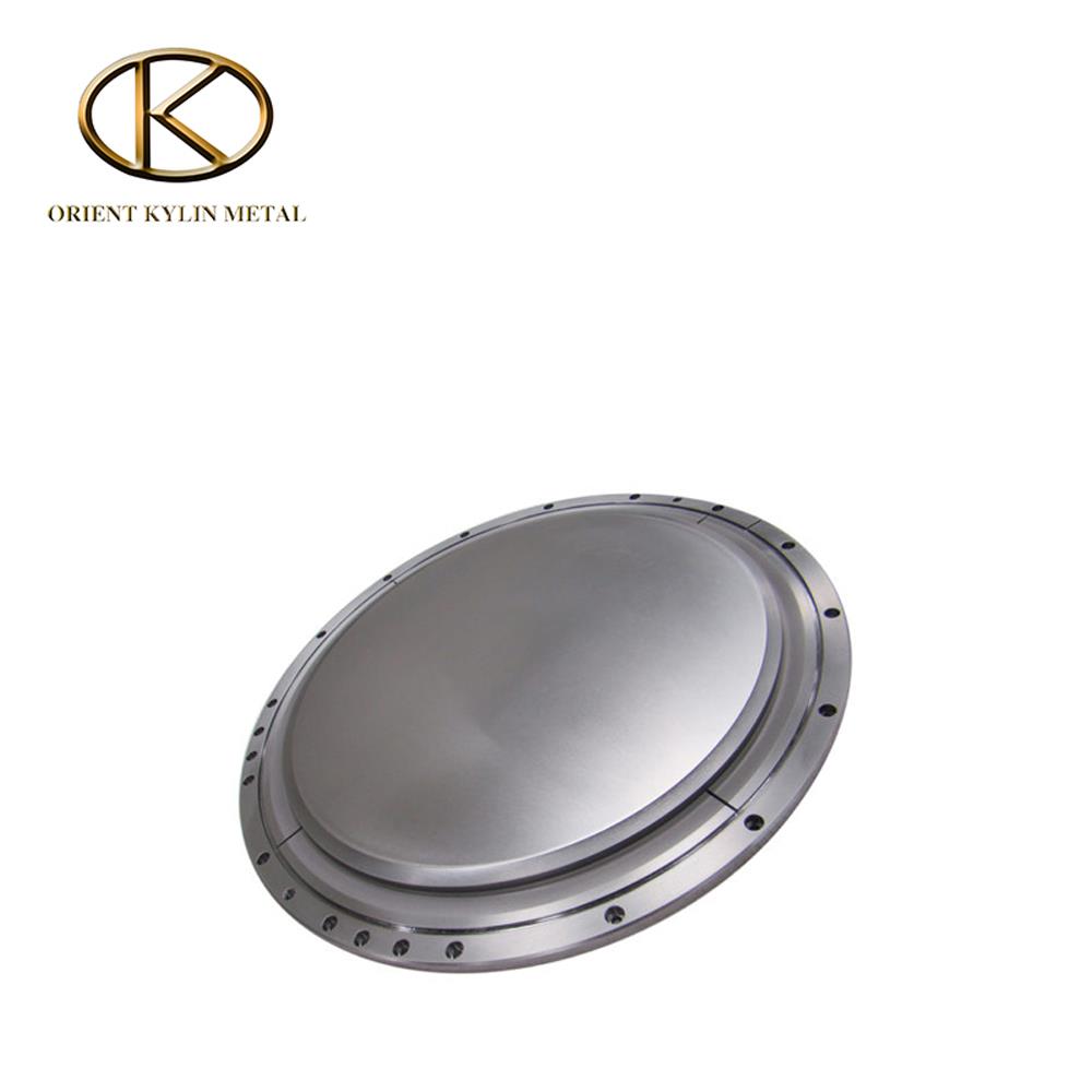
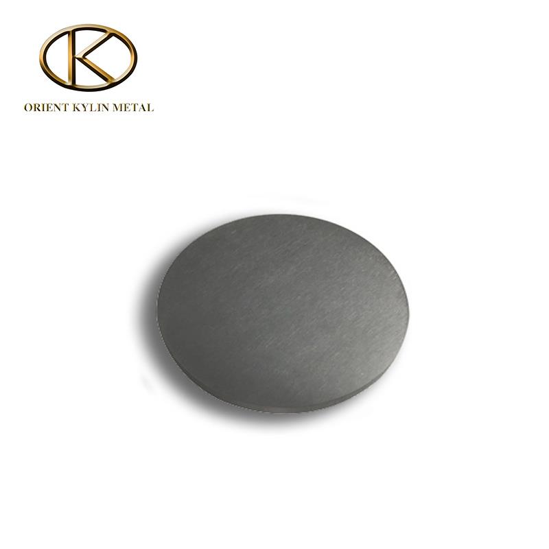
Tantalum Sputtering Target for Semiconductor Applications
This tantalum sputtering target is designed for semiconductor applications requiring thin film deposition. It provides a uniform and consistent tantalum layer.
Technical Specifications
Product Overview
High-Purity Tantalum Sputtering Solutions
These tantalum sputtering targets are engineered specifically for demanding semiconductor and micro-electronics applications. Produced via vacuum electron beam melting, they offer exceptional density and a uniform microstructure to ensure constant erosion rates and homogeneous layer deposition. With high natural strength and a low thermal expansion coefficient, these targets serve as an ideal diffusion barrier between copper and silicon.
Material Properties
- Material
- High-purity steel gray tantalum metal
- Physical Characteristics
- DuctileVery HardHigh DensityRefractory MetalHigh Thermal ConductivityHigh Electrical Conductivity
- Corrosion Resistance
- Immune to normal aqua regia at temperatures below 150°C
Technical Specifications
Typical Purity
3N5 (99.95%)High Purity
Analytical Methods
- Metallic elements: GDMS and ICP-OES
- Gas elements: LECO
- Manufacturing Process
- Vacuum Electron Beam (EB) Melting
Applications
- Primary Industries
- SemiconductorsMicro-electronicsThin Film ResistorsMagnetic Recording MediaFlat Panel DisplaysOptics
Manufacturing Workflow
Production Sequence
- Sintering of high-purity powder
- Vacuum Electron Beam Melting
- Plastic Deformation
- Annealing
- Metallographic Inspection
- Machining & Dimensional Inspection
- Cleaning & Final Packaging
Available Alloys
- Other Alloy Forms
- Tantalum TungstenTantalum NiobiumTantalum AluminumTantalum SiliconTantalum Hafnium