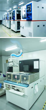
Wafer Thinning System for Semiconductor Manufacturing
This advanced wafer thinning system is designed for precision semiconductor manufacturing. It utilizes state-of-the-art technology to achieve uniform and controlled material removal, ensuring optimal wafer flatness and thickness.
Technical Specifications
Overview
Precision Thinning Capability
This advanced wafer thinning system is engineered for high-precision semiconductor manufacturing, delivering uniform material removal across diverse wafer sizes and materials. The equipment integrates automated handling and real-time process monitoring to ensure superior flatness, optimized thickness, and consistent high yields. Designed for efficiency and safety, it features a intuitive user interface and robust interlock systems to support seamless high-throughput operations.
Technical Capabilities
Operational Features
- Automated wafer handling
- Real-time process monitoring
- Precision material removal
- Comprehensive safety interlocks
System Performance Metrics
1 High
Throughput Level
1 Automated
Operation Mode
Compliance and Standards
- Certifications
- Industrial GradeSafety Certified