Package Substrates
Source high-performance package substrates from vetted manufacturers and suppliers. Designed for importers, distributors, procurement managers, and electronics brands requiring reliable OEM production in volume. Secure competitive wholesale pricing on precision IC substrates built to your exact thermal and electrical specifications.
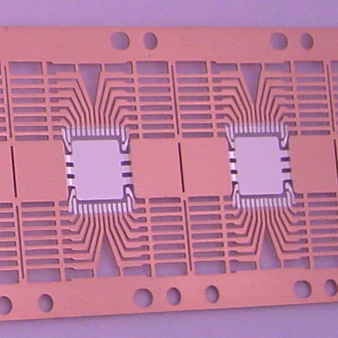
Package substrates are the critical interface between the bare semiconductor die and the system printed circuit board (PCB). Sourcing these components at scale requires navigating tight tolerances, advanced material selections, and stringent defect controls. For high-density interconnect (HDI) and IC packaging applications, the margin for error is zero.
Core Specifications and Material Selection
Choosing the right substrate material dictates the thermal and electrical performance of the final IC package. The material must offer a Coefficient of Thermal Expansion (CTE) that bridges the gap between the silicon die and the motherboard to prevent solder joint fatigue.
| Material | Primary Use Case | Key Characteristics |
|---|---|---|
| BT Resin (Bismaleimide Triazine) | Memory, LED, standard BGA | Excellent thermal stability, highly reliable, high Tg. |
| ABF (Ajinomoto Build-up Film) | CPU, GPU, Flip-Chip (FC) | Ideal for ultra-fine line routing and high layer counts. |
| Polyimide (PI) | Flexible packaging (COF, TAB) | High flexibility, excellent heat resistance, thin profile. |
Line width and spacing (L/S) are equally critical. Advanced flip-chip substrates routinely push L/S down to 10/10 micrometers or lower, demanding state-of-the-art semi-additive processes (SAP) rather than standard subtractive etching.
Need a supplier capable of SAP and ultra-fine L/S? Let us match you with a vetted manufacturer.
Talk to our teamManufacturing Yield and Quality Control
Yield is the primary driver of cost in IC substrate manufacturing. Because package substrates require significantly finer geometries than standard PCBs, microscopic dust or minor process variations can cause catastrophic shorts or opens.
Critical Factory Audit Points for Substrate Suppliers
- Class 100 or Class 1000 cleanroom environments for imaging and plating.
- Advanced automated optical inspection (AOI) calibrated for ultra-fine L/S.
- Laser drilling capabilities for microvias under 50 micrometers.
- Strict environmental controls to prevent moisture absorption and subsequent delamination.
Validating a factory's true capabilities before tooling begins is essential. A rigorous factory audit ensures the supplier actually owns the high-end equipment they claim, rather than outsourcing your critical layers to unverified sub-tier vendors. Furthermore, implementing robust quality control and inspection protocols—specifically focusing on warpage control, via reliability, and surface finish integrity—prevents defective batches from leaving the facility.
Pricing, Tooling (NRE), and MOQs
The economics of package substrates differ significantly from standard rigid PCBs. Buyers must account for upfront engineering costs and facility utilization requirements.
- NRE and Tooling: Non-recurring engineering (NRE) costs are substantial. Electrical testing fixtures, laser direct imaging (LDI) setups, and custom tooling often run into the thousands of dollars depending on layer count and via structure.
- MOQs: For mass production, factories typically set minimum order quantities based on panel utilization. Expect MOQs starting around 5,000 to 10,000 pieces for standard BGA substrates, though high-value flip-chip substrates may have lower volume thresholds negotiated based on total contract value.
- Lead Times: Standard lead times range from 4 to 6 weeks for established designs, but raw material shortages (particularly for specialized ABF films) can stretch timelines to 10 weeks or more.
Struggling with high NRE costs or inflexible MOQs? We negotiate terms that align with your production schedule.
Get a free consultationFrequently Asked Questions
Securing a reliable supply of package substrates requires more than just sending Gerber files to a manufacturer. It demands active oversight of material sourcing, yield rates, and quality protocols. By partnering with experienced product sourcing professionals, you ensure your IC packaging lines run without interruption, backed by verified suppliers capable of meeting your exact technical demands.
Get Sourcing Help for Package Substrates
Tell us your requirements and our experts will connect you with verified manufacturers.