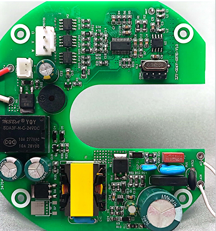
Double-Sided PCB
Source double-sided PCBs from vetted manufacturers and suppliers to meet your exact specifications. Designed for electronics importers, distributors, and brands requiring reliable OEM production, our wholesale double-sided printed circuit boards deliver high-density routing and superior electrical performance for volume manufacturing.
Double-sided printed circuit boards (PCBs) form the backbone of modern consumer and industrial electronics, offering a critical balance between routing density and manufacturing cost. Sourcing these boards in volume requires strict alignment with a factory's fabrication capabilities, particularly regarding through-hole plating reliability, trace tolerances, and substrate material consistency.
Critical Specifications for Volume Production
When moving from prototyping to bulk production, matching your Gerber files and fabrication notes to the right supplier's standard operating window is essential to avoid yield drops and cost overruns.
Substrate Selection and Thermal Performance
The majority of double-sided boards utilize FR4, but specifying the correct Glass Transition Temperature (Tg) is vital based on the end-use environment and assembly process. Standard Tg (around 130 to 140 degrees Celsius) is sufficient for basic consumer electronics, while High-Tg (170 degrees Celsius and above) is required for automotive, industrial, or multi-pass RoHS-compliant reflow assembly. Failing to specify the correct Tg can lead to barrel cracking in plated through-holes (PTH) or pad lifting during assembly.
Need help matching your PCB specifications with a capable, high-yield manufacturer?
Talk to our teamSurface Finishes and Fabrication Quality
The surface finish protects exposed copper from oxidation and provides a solderable surface for assembly. The choice of finish directly impacts shelf life, assembly yield (especially for fine-pitch components), and unit cost.
| Finish Type | Relative Cost | Shelf Life | Ideal Application |
|---|---|---|---|
| HASL (Lead-Free) | Baseline | 12 Months | General electronics, larger pitch |
| ENIG | High | 12 Months | Fine pitch components, wire bonding |
| OSP | Low | 6 Months | High-volume, rapid assembly cycles |
| Immersion Silver | Moderate | 6 to 12 Months | High-frequency signals, flat pads |
Defect Prevention on the Factory Floor
Quality is won or lost during the chemical plating and etching processes. Relying on end-of-line testing is not enough; you must ensure the factory has robust in-process controls. Executing thorough Factory Audits before placing large POs ensures the supplier maintains the necessary equipment and process controls.
Key Factory Capabilities to Verify
- Automated Optical Inspection (AOI) utilized after etching to catch shorts and opens.
- 100 percent Electrical Testing (E-Test) using flying probe for small runs or bed-of-nails fixtures for volume.
- Microsection analysis capabilities to verify copper plating thickness inside through-holes.
- Strict chemical bath monitoring for the electroless copper plating line.
If you are managing complex runs, implementing independent Quality Control & Inspection prior to shipment is critical to catch cosmetic defects, solder mask misalignment, or warping before the boards leave the facility.
Wholesale Pricing, MOQs, and Lead Times
Pricing for double-sided PCBs is highly commoditized but sensitive to panel utilization. Factories manufacture boards on standard panel sizes (such as 18 by 24 inches). If your board dimensions do not panelize efficiently, you will pay for wasted FR4.
- Tooling and NRE: Non-Recurring Engineering (NRE) and electrical test fixture costs are typically charged on the first run. For high-volume orders, many factories will amortize or waive these fees.
- MOQs: While prototype shops have no minimums, true volume manufacturers typically require minimum orders of 5 to 10 square meters of board material to achieve optimal pricing.
- Lead Times: Standard production lead times for double-sided boards range from 8 to 14 days after Gerber approval, excluding shipping. Peak seasons or material shortages (like copper foil constraints) can push this to 3 to 4 weeks.
Optimize your panelization and secure better wholesale pricing for your PCB runs.
Get a free consultationFrequently Asked Questions
Successfully sourcing double-sided PCBs at scale requires more than just sending Gerber files to the lowest bidder. It demands a clear understanding of material specifications, panel efficiency, and factory quality systems. Partnering with a professional Product Sourcing team ensures your designs are matched with the right tier of manufacturer, protecting your assembly yields and your bottom line.
Get Sourcing Help for Double-Sided PCB
Tell us your requirements and our experts will connect you with verified manufacturers.